To investigate the use of a bypass (decoupling) capacitor on suppressing power supply voltage fluctuation for a digital IC.
To use SPICE to compare measured results with that of a simplified circuit model.
2. Equipment
Two channel oscilloscope (an oscilloscope with a bandwidth of at least 50 MHz or above is preferable).
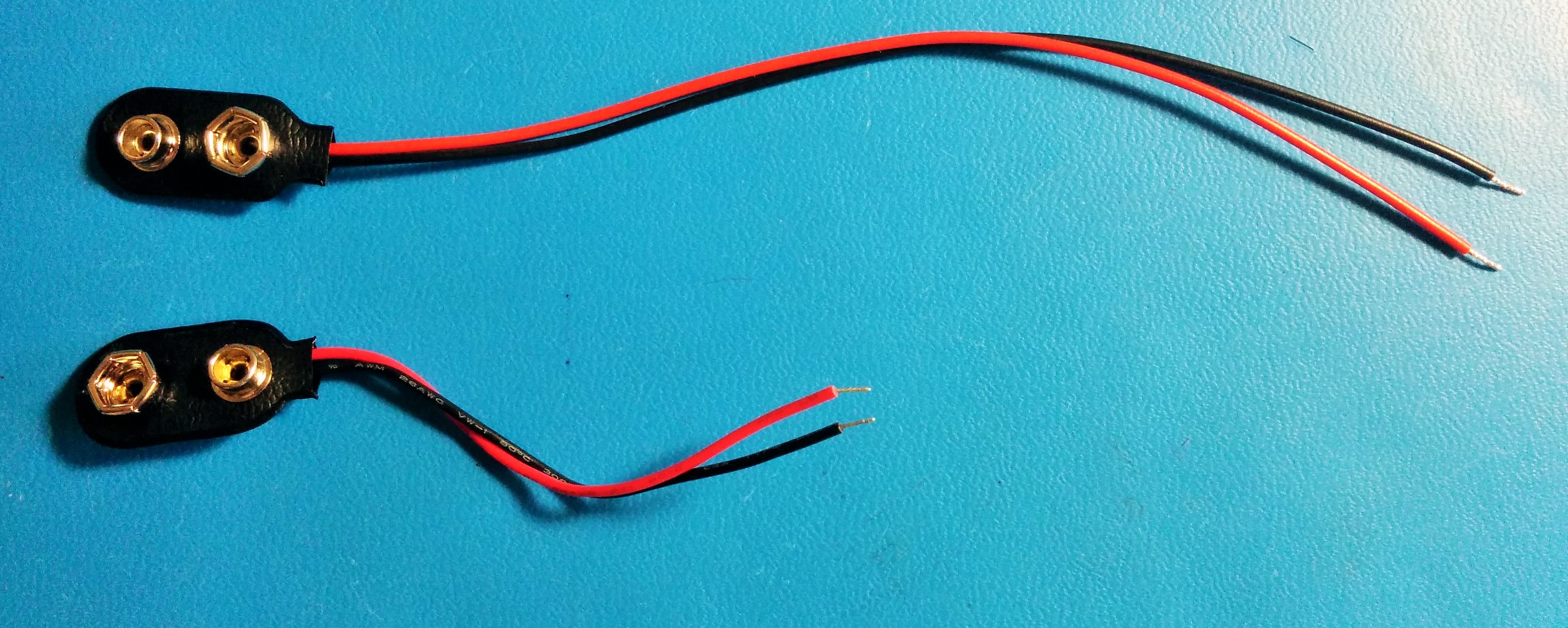
Two 9V battery leads: One short set of leads (around 3 inches) and one long set of leads (around 6 inches).
See picture of leads here.
One standard breadboard
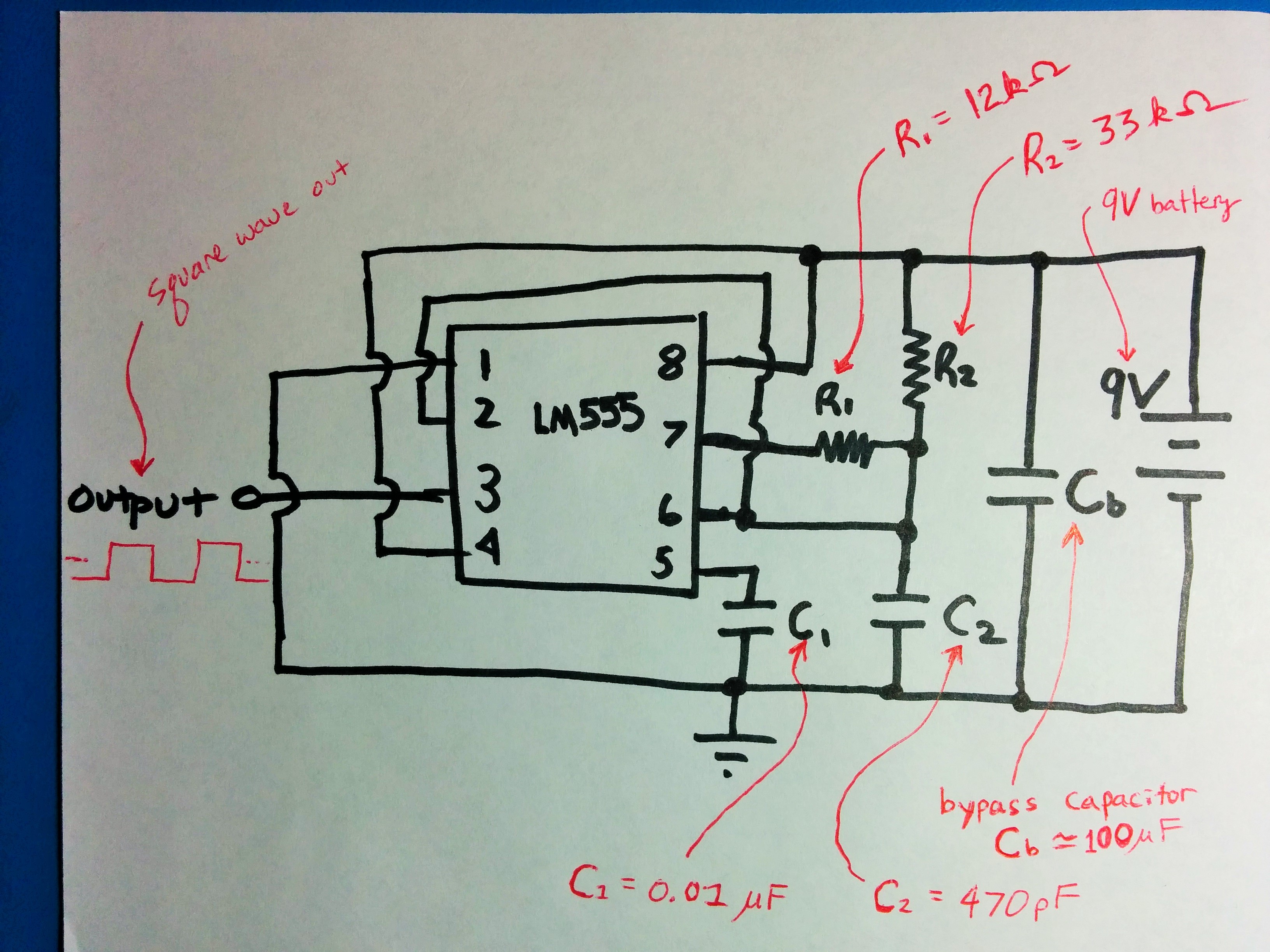
Capacitors: four 470 pF, four 0.01 uF, one .01 uF, one 1uF, one 10 uF, two 100 uF.
Resistors: one 4.7 Ohm, two 12 kOhm, two 33 kOhm
22 gauge wire for simple breadboard wiring.
Wire cutters/strippers.
Needle nose pliers for conveniently connecting wires to breadboard.
3. Report guidelines
For the lab report, you will create a PowerPoint presentation (or use a similar presentation program), save it as a PDF, and
submit it on-line according to the instructions given in class. The presentation should be tutorial in nature; your target audiences are
other engineers and scientists who are interested in learning more about circuits and electromagnetism.
Your presentation will have 27 slides. Please include a slide number in the footer of each slide. To earn full credit your presentation must
contain the slides in the order asked for in this lab. If you miss a slide, please leave a blank slide in its place so that you have
still have exactly 27 slides total. Your first two slides should be:
Slide 1: Title slide with our name, student ID number, date, lab name, class number/title.
Slide 2: A team picture or insignia with the names of your teammates.
4. Procedure
4.1 Construct and test the LM555 square-wave oscillator
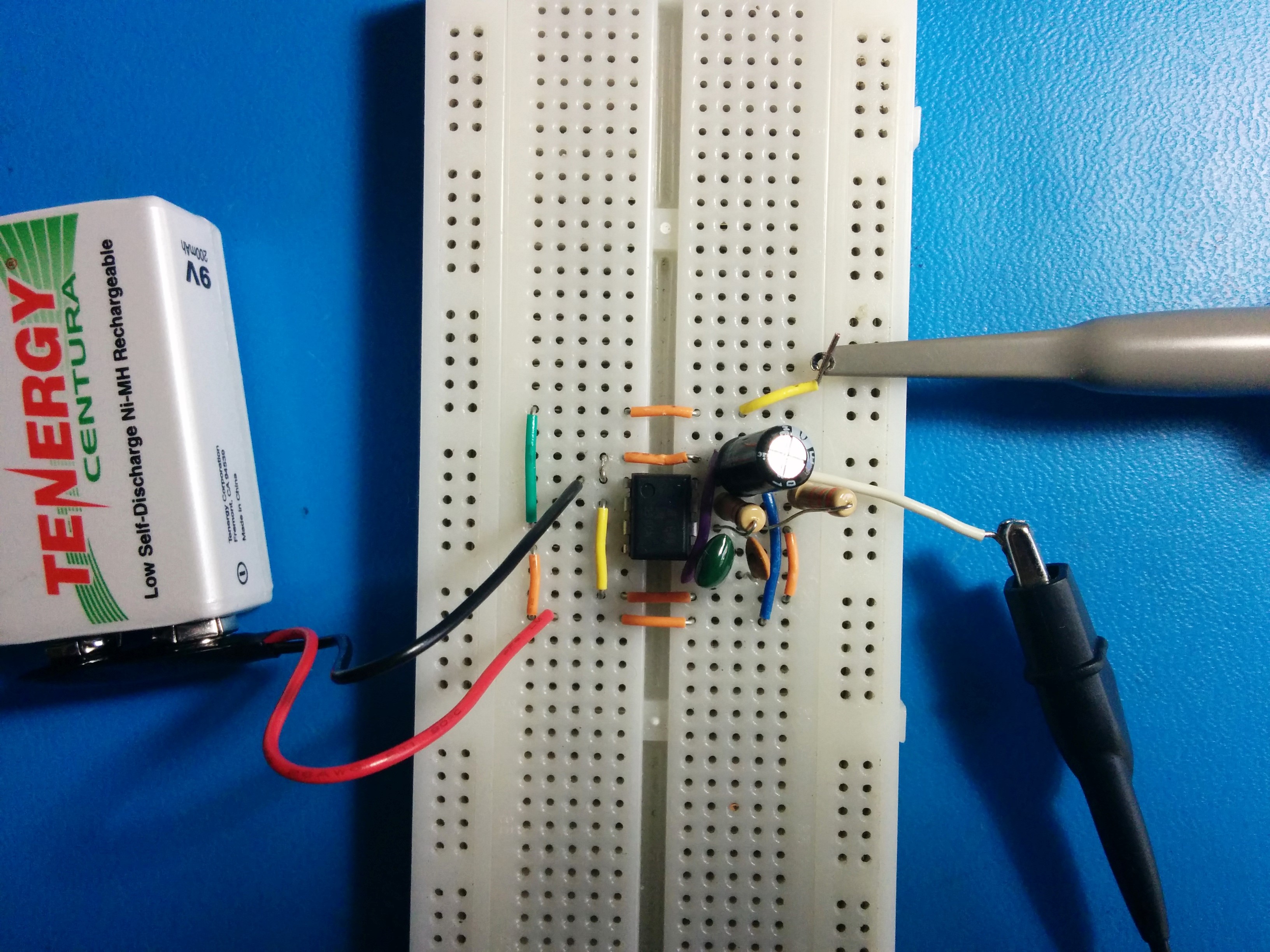
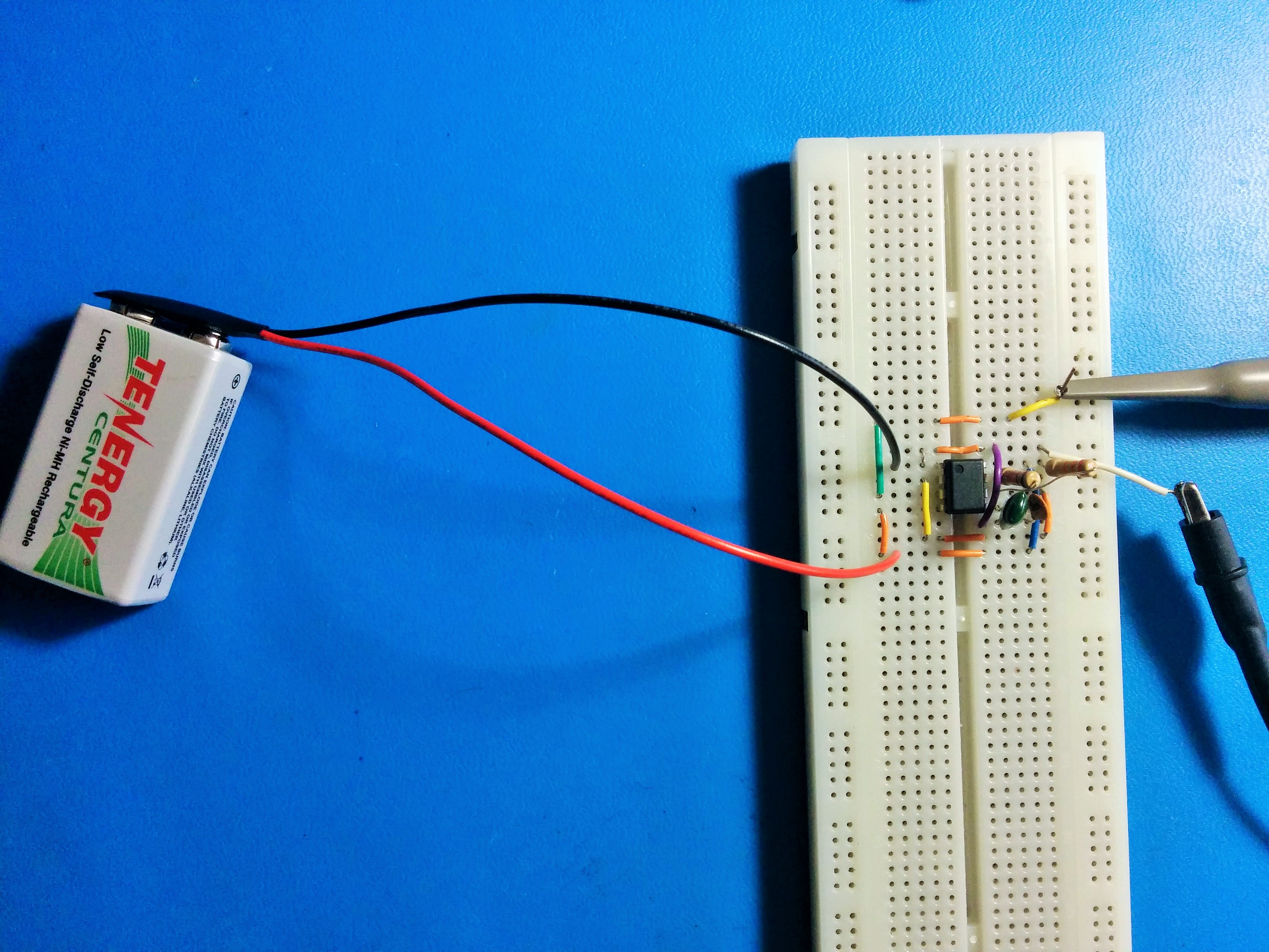
Build your LM555 square-wave oscillator on a breadboard according to the circuit schematic in Figure 1.
Be sure to follow good wiring practice, meaning keep your circuit compact, neat, and orderly. If given a choice, use short component leads instead of long leads.
This means clip off excess wire on the resistor and capacitor leads so the components fit neatly in the circuit. Also, try to keep wires and components flat on the board.
You want to avoid your circuit looking like a disorderly tangle of wires (rat's nest). Also, because this circuit is so simple, you don't
need to use the ground and power rails of the breadboard. Note that the equipment list includes both short and long 9V battery leads.
For this circuit, please use the shorter of the two sizes of 9V battery leads. Remember to double check your wiring before applying power.
Figure 2 shows a photograph of a 555 square wave oscillator circuit implemented with decent wiring practice.
Present a photograph of your circuit in Slide 3.
Figure 1. Schematic of LM555 square wave oscillator.
Figure 2. Photograph of LM555 square wave oscillator.
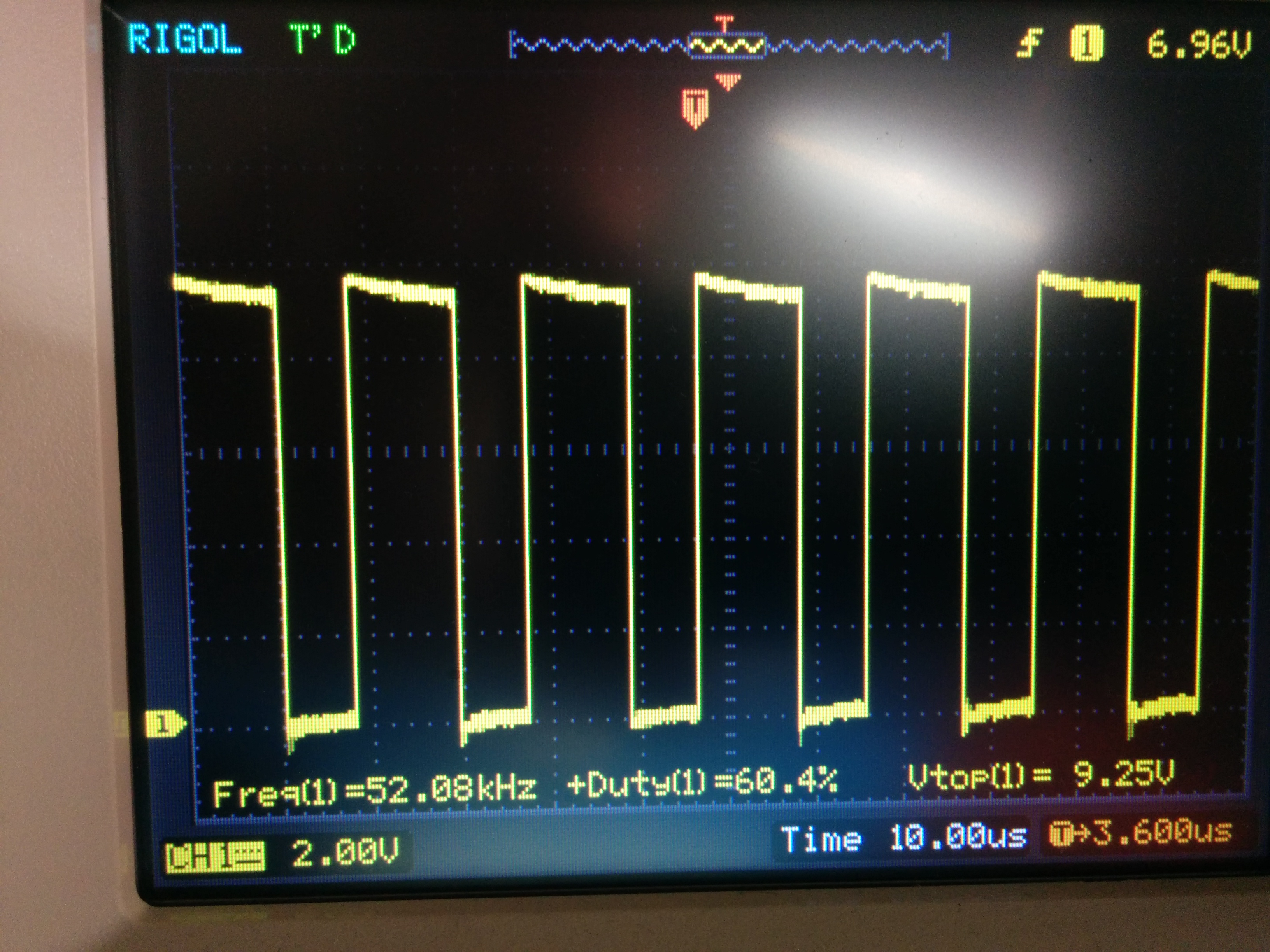
Using an oscilliscope, measure the output voltage of the oscillator with respect to ground (the probe tip should be connected to measure the IC's signal output and the probe's ground clip should be connected to IC ground.)
You should see a pulse train as shown in Figure 3. If you don't observe this, go back and recheck the connections in your circuit and/or replace the battery/LM555.
Figure 3. Output voltage of square wave oscillator with respect to ground.
4.2 Bypass capacitor's effect on output voltage
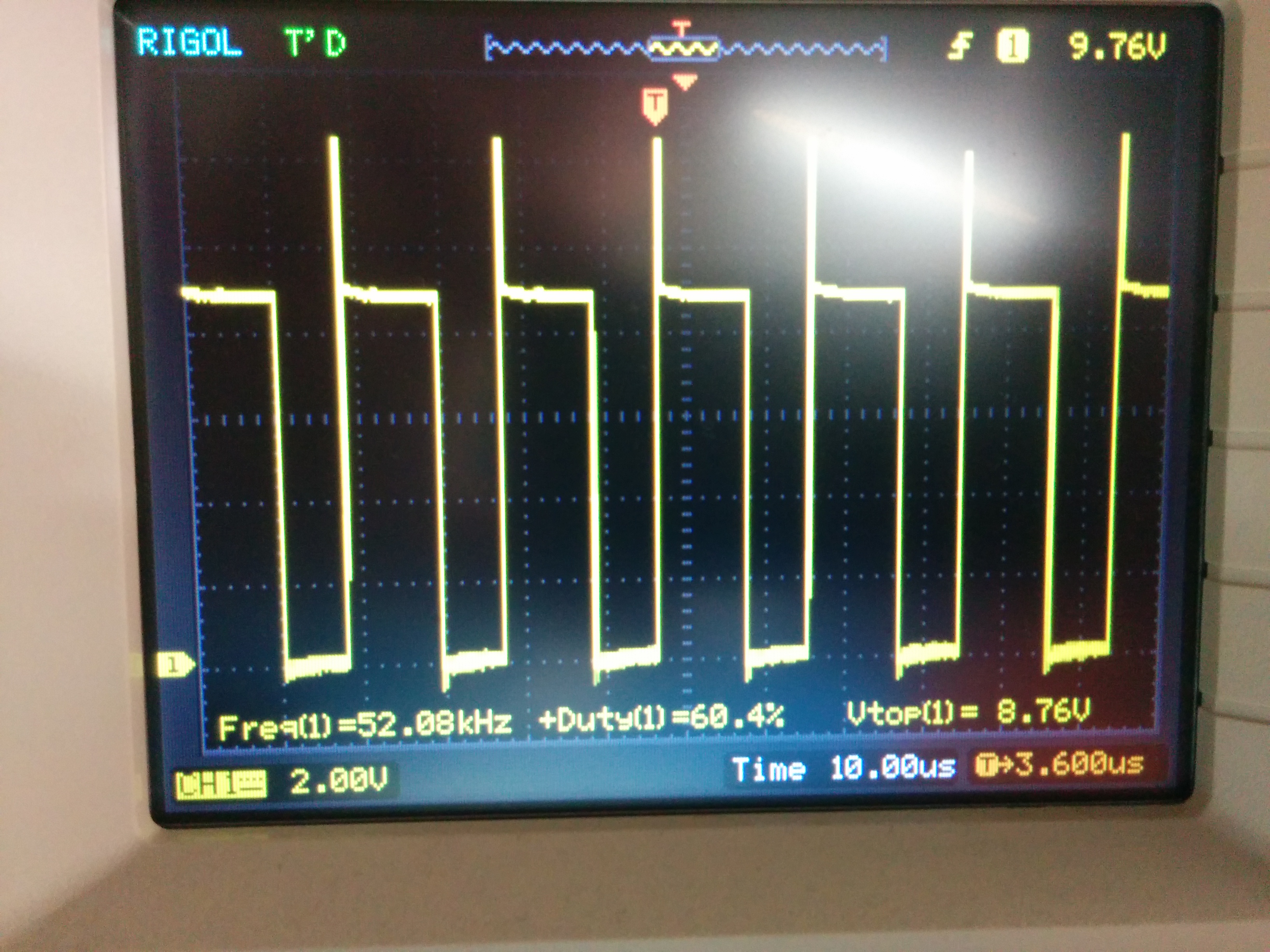
Now remove the 100uF bypass capacitor (i.e. keep the the same configuration as Figure 1, but don't include the bypass capacitor Cb),
and the output voltage of the oscillator should now exhibit a big overshoot (with possible ringing) on the rising edge of each pulse in the pulse train,
like that shown in Figure 4.
Figure 4. Output voltage of square wave oscillator with respect to ground. No bypass capacitor.
Replace the bypass capacitor,
and adjust the vertical and horizontal scale of the oscilloscope to zoom in on a rising edge of a pulse for a better
view of the signal in this region. Measure the rise time and the maximum voltage (Vmax). Take a screenshot with the oscilloscope (a photograph of the oscilloscope's screen works fine, too).
Present both the measured rise time and screenshot in Slide 4.
Remove the bypass capacitor and take a screenshot (you may need to readjust the zoom to focus again on a rising edge).
How does the absence of the bypass capacitor effect the shape and Vmax of the rising edges of the output square wave? Present your answer to this question and the
screenshot in Slide 5.
Replace the bypass capacitor, and zoom in on the falling edge of a pulse in the output pulse train. Measure the fall time and take a screenshot.
Present the measured fall time and screenshot in Slide 6.
Now remove the bypass capacitor,
and take a screenshot of the falling edge. How does the absence of the bypass capacitor effect the falling edges of the output pulse train?
Present your answer to this question and screenshot in Slide 7.
4.3 Bypass capacitor's effect on the quality of power supply voltage
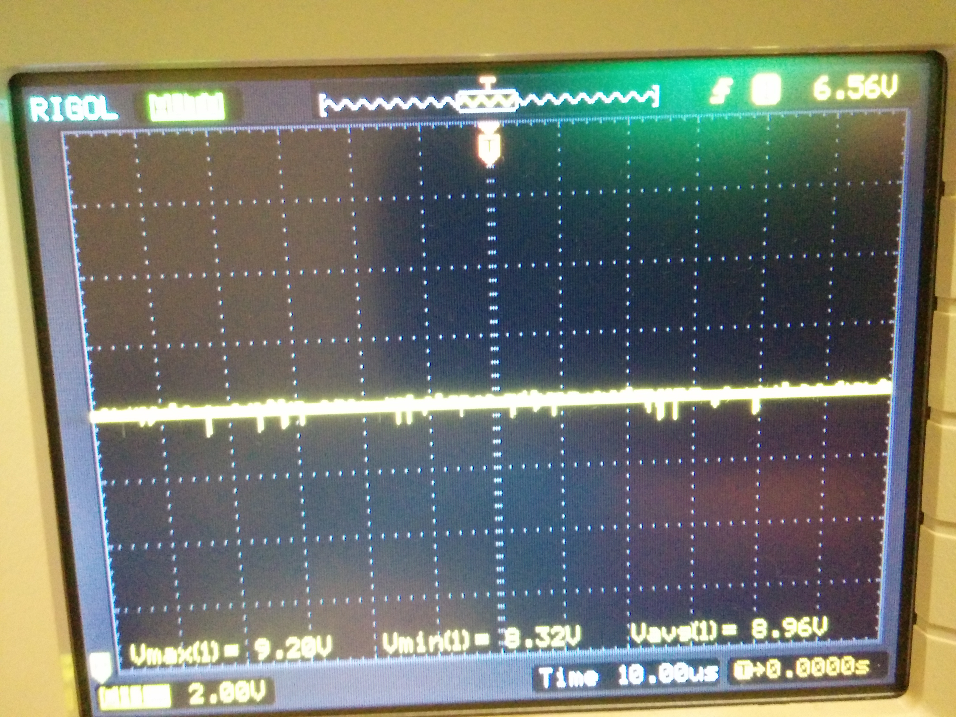
Replace the bypass capacitor and connect the oscilloscope probe to measure the voltage of the power pin (pin number 8) of the LM555
with respect to ground. You should see a relatively "clean" supply voltage centered at around 9 V (some low-amplitude voltage spikes will likely be present), like that shown in Figure 5 below. Take a screenshot and present it in Slide 8
Figure 5. Supply voltage with bypass capacitor.
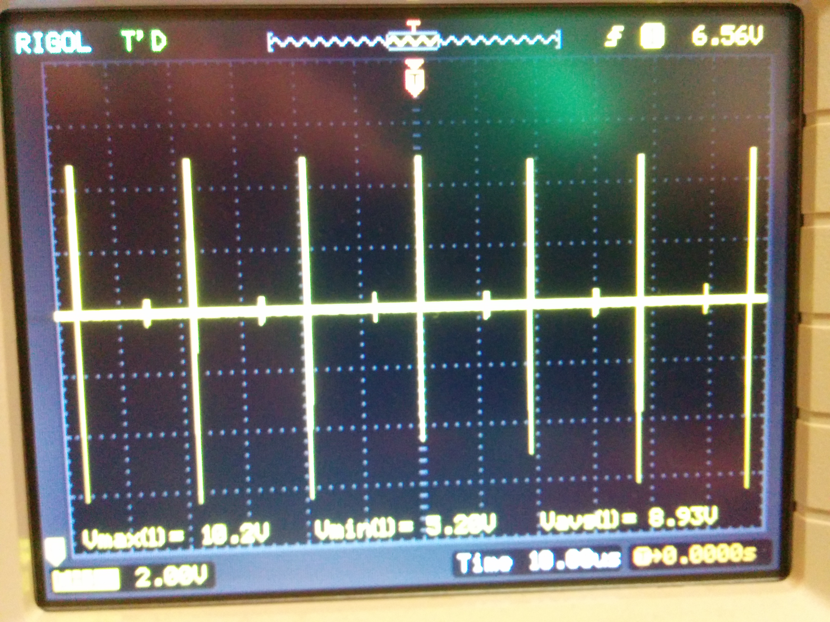
Remove the the bypass capacitor, and observe the effect on the power supply voltage. You should now see regular perturbations or "spikes" in the voltage, like that shown in Figure 6 below.
Figure 6. Supply voltage without bypass capacitor.
With the bypass capacitor still removed, adjust the vertical and horizontal scales of the oscilloscope to zoom in for a closer look at one of the big voltage spikes on the power supply.
Take a screenshot and present it in Slide 9.
With the bypass capacitor still removed, use the two channels of the oscilliscope to simultaneously probe the output signal and the power supply.
Do the big spikes on the power supply occur during the rising or falling edges of the square wave output signal?
Present your answer to this question with any supporting screenshots in Slide 10.
4.4 Power supply lead length's effect on output signal and supply voltage
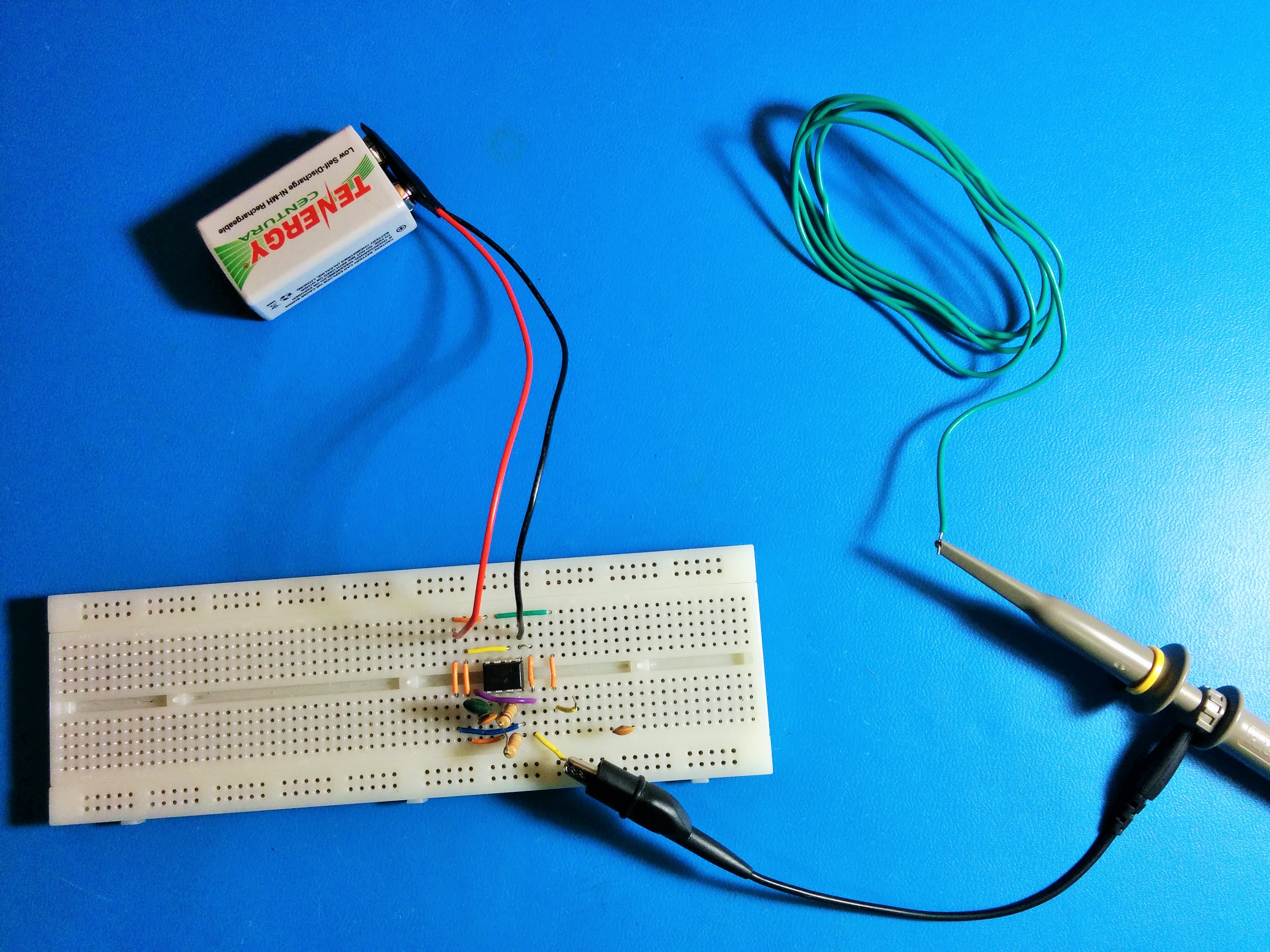
If it's not removed already, remove the bypass capacitor from the oscillator. Now, replace the short 9V battery leads with the longer leads, as shown in Figure 7.
Warning: Be careful when working with long leads; it's easy for them to accidently short together when they are not plugged into the breadboard.
If you smell something funny, immediately check that your battery isn't shorted and melting.
Figure 7. Photograph of LM555 square wave oscillator with longer 9V battery leads. Bypass capacitor removed
Using an oscilloscope, measure the output of the oscillator (which has the long 9V leads). In this measurement there should be no bypass capacitor (the bypass capacitor should be have been removed in previous step).
Does having longer battery leads effect the output voltage? If it does, how so?
Along with your observations, please present any supporting oscilloscope measurements and/or screenshots in Slides 11. Feel free to go back and remeasure the output with shorter leads to make a
good comparison between the two lead lengths in your presentation.
Perform the same comparison as in the previous step, except measure the voltage on the IC power pin (instead of the output voltage as in the previous step).
Does having longer battery leads effect the voltage on the power pin? If it does, how so?
Along with your observations, please present any supporting oscilloscope measurements and/or screenshots in Slide 12.
As before, feel free to go back and remeasure the output with shorter leads to make a
good comparison between the two lead lengths in your presentation.
4.5 Bypass capacitor's effect on power supply as a source of electromagnetic interference (EMI)
With a piece of long wire, construct a crude wireless sensing coil and attach one end to the oscilloscope probe as shown in Figure 8.
The probe's ground clip should be connected to the ground pin of the IC. Place the probe a few inches away from the long battery leads
as shown in the figure.
Measure the probe voltage near the oscillator with and without the bypass capacitor.
How does the bypass capacitor effect the measured voltage? What does this say about the
bypass capacitor's effect on the power supply as a source of EMI in general? Present your observations
and screenshots in Slide 13.
Figure 8. Photograph of oscilloscope probe with sensor coil. Bypass capacitor removed
4.6 Bypass capacitor's effect on surges in power supply current
Start with the same oscillator circuit as shown in Figure 7 (oscillator with long 9V battery leads
and bypass capacitor removed.)
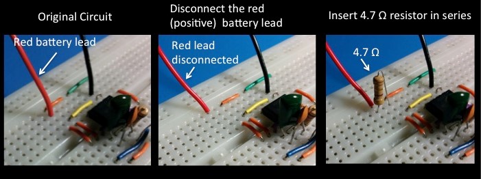
We will now set up the oscilloscope to measure the current through the battery using the series of steps presented in Figure 9. The first step is to disconnect the positive (red) battery lead from the circit, while leaving the
black lead connected to system ground. Next, connect a small resistor (such as a 4.7 Ohm resistor) in series with the positve
battery lead and the circuit. Finally, connect the oscilloscope probe
and it's groud lead to measure the voltage across the 4.7 Ohm resistor. ACTUALLY, BEFORE YOU CONNECT THE OSCILLISCOPE BE SURE YOU ARE USING
A BATTERY FOR A POWER SOURCE AND NOT A BENCH TOP POWER SUPPLY (see warning below). By simple Ohm's Law, the current through the
resistor is equal to Vmeas/Rmeas where Vmeas is the measured voltage using the oscilloscope and Rmeas is the actual (measured) resistance of the
4.7 Ohm resistor. Warning: This is a differential or "floating" measurement, meaning we are using the oscilloscope to find the voltage across a series element.
Normally, you would not use a traditional oscilloscope/probe to make such a measurement, because the oscilloscope has it's "signal common" terminal
connected to the protected grounding system, i.e. "earth ground". However, in this case we are able to make this measurement, because the oscillator is powered by a battery, which does not have its ground connected to Earth Ground. For more information
on this topic, check out this Technical Brief by Tektronix.
Figure 9. Setup to measure power supply current.
Using the setup described above, measure the current through the battery without the bypass capacitor. You will observe distinct current pulses. Adjust the horizontal and
vertical scales of the oscilloscope to zoom onto a single pulse.
What is the duration of one current pulse in nanoseconds? What is the maximum amplitude of the pulse?
Does the current pulse correspond to a rising or falling edge of the output signal pulse train. Take a screenshot. Present your answer, measurements
and screenshot in Slide 14.
Replace the bypass capacitor and measure the current through the battery. You will observe that the current pulses decrease significantly in amplitude.
Agian, adjust the horizontal and
vertical scales of the oscilloscope to zoom onto a single pulse and take a screenshot.
What is the maximum amplitude of the pulse now?
Present your measurement
and screenshot in Slide 15.
4.7 What size of bypass capacitor should I choose?
Start with the same oscillator circuit as shown in Figure 7 (oscillator with the long 9V battery leads
and bypass capacitor removed.) Make sure the 4.7 Ohm resistor we inserted in the previous section (Section 4.6) is removed.
Connect the oscilloscope probe to the power pin (pin number 8) of the LM555, and measure the voltage at this pin with respect to ground.
You should now see regular perturbations or "spikes" in the voltage, like that shown in Figure 6 in section 4.3.
With the bypass capacitor still removed, adjust the vertical and horizontal scales of the oscilloscope to zoom in for a closer look at
one of the big voltage spikes on the power supply.
Measure and compare the maximum amplitude of the voltage spikes
for five different valued bypass capacitors: 470 pF, 0.01 uF, 1 uF, 10 uF, 100 uF.
How does the size of bypass capacitor effect the "quality" of supply voltage (i.e. suppresses the voltage spikes)? Present your measurements and observations in
in Slide 16
Instead of one bypass capacitor as before, try using two bypass capacitors in parallel from the values you have in the step above.
For example, measure the supply voltage using a 470 pF bypass capacitor in parallel with a 100 uF bypass capacitor.
Or you can try two 100 uF capacitors in parallel. Is there a certain optimum combination you found with respect to suppressing the voltage spikes?
Present your measurements and observations in Slide 17.
4.8 Interference with other circuits
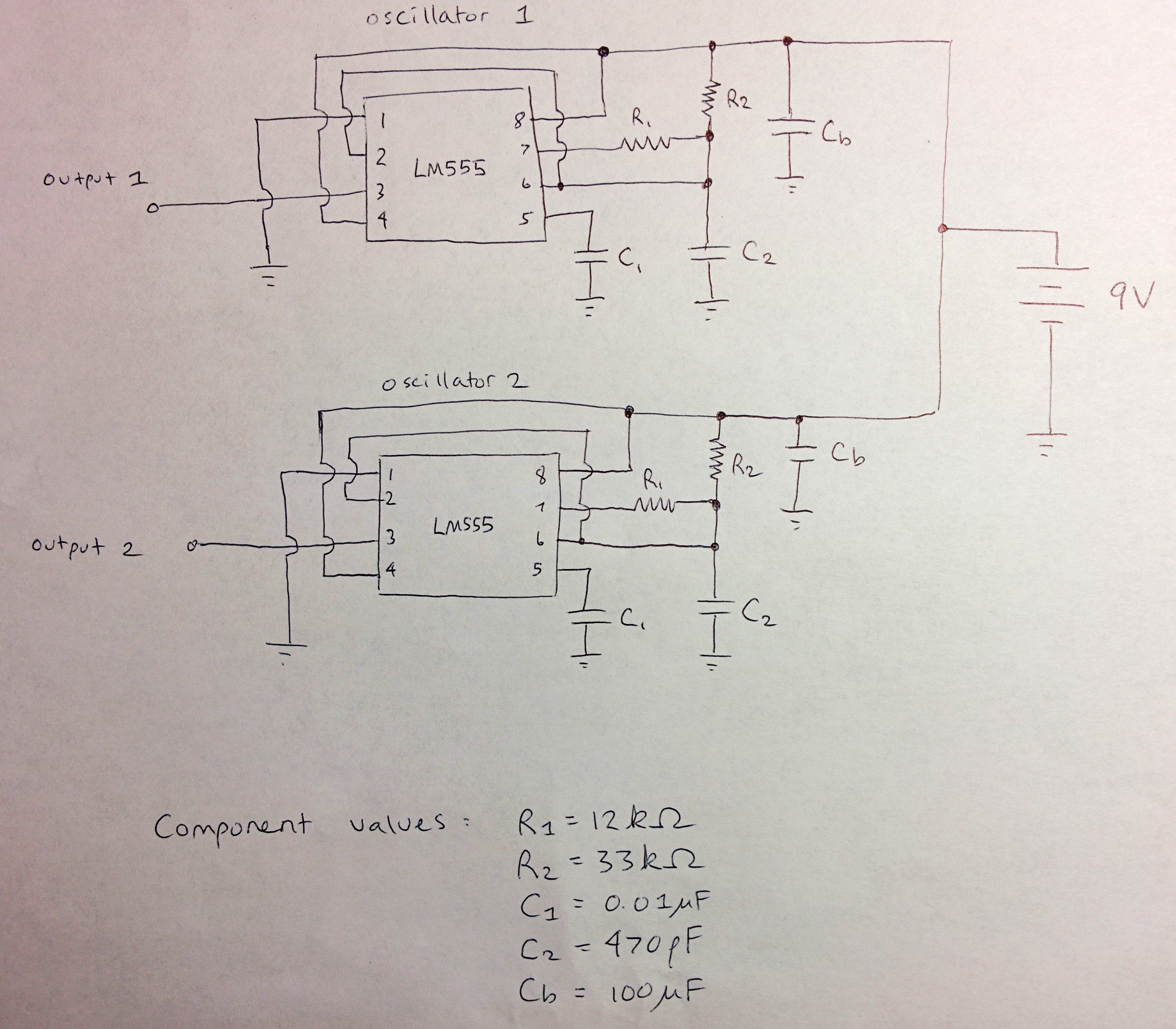
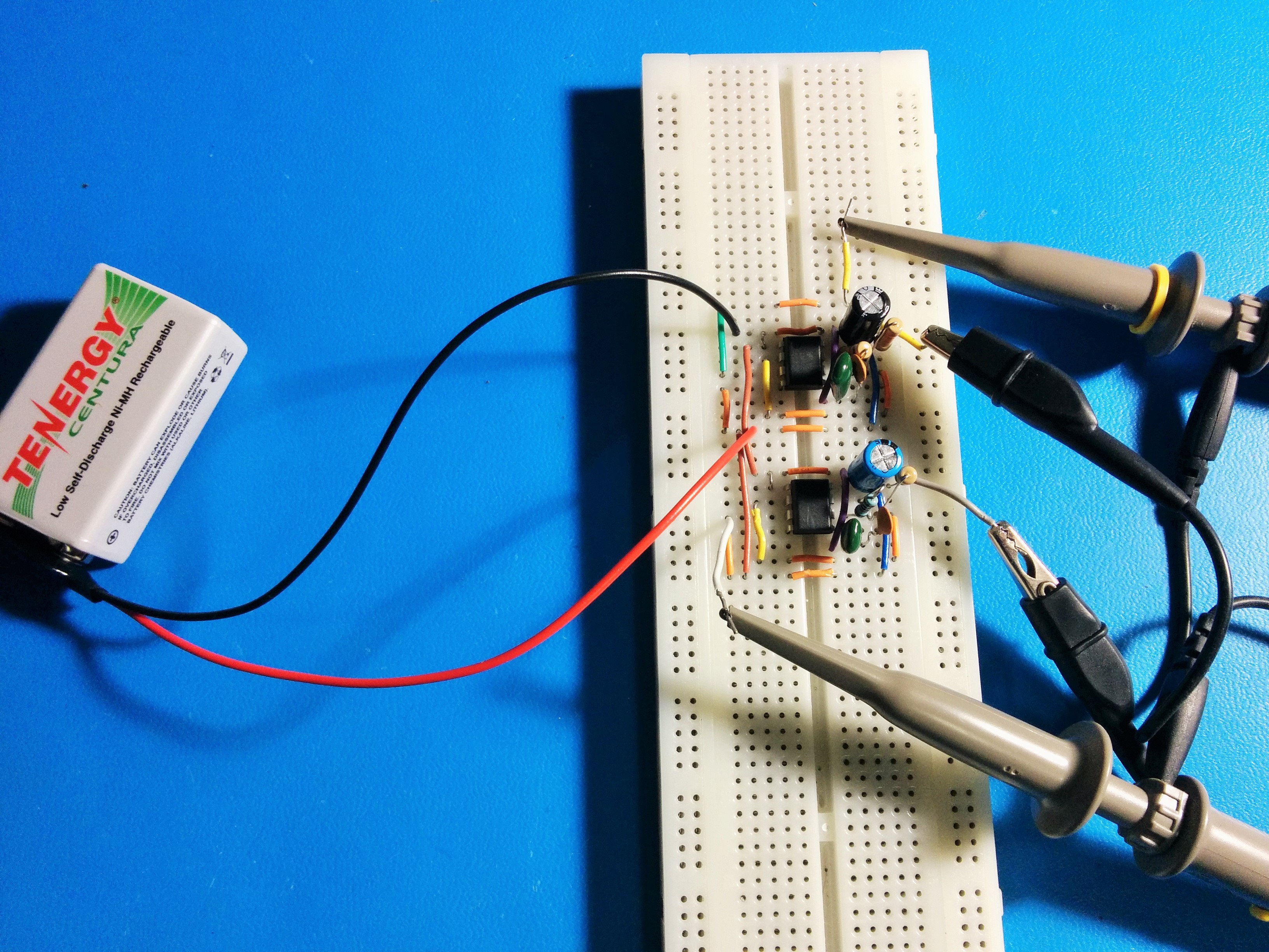
Construct a second oscillator with the same component values as the first. Both oscillators should share the same ground and
power supply. A schematic and photograph of the two-oscillator system is shown in Figures 10 and 11, respectively.
Figure 10. Schematic of the two oscillators.
Figure 11. Photograph of the two oscillators.
Use the two channels of the oscilloscope to measure and display the output signals for both oscillators simultaneously.
Make sure each oscillator has its own local bypass capacitor.
Take a screenshot with the oscilloscope. The screenshot should contain two relatively "clean" pulse trains with
similar frequencies and duty cycles. Because of component tolerance, there will be some differences between
the two output signals, and they will be almost certainly out of phase. Based on the output waveforms, do the oscillators seem coupled or decoupled? Meaning, do the oscillators operate independently from one another (decoupled)
or does the operation of one seem to effect the operation of the other (coupled)? Present your answer and screenshot in slide Slide 18.
Now remove the bypass capacitors.
Take a screenshot with the oscilloscope. The screenshot should contain two pulse trains,
which are both corrupted by large fast voltage spikes.
Is the output of an oscillator in this double-oscillator system (without bypass capacitors) more or less corrupted by voltage spikes than the output of a single, isolated
square wave oscillator (without a bypass capacitor)?
What is the root cause of the voltage spikes?
Without bypass capacitors, would you say the oscillators are coupled or decoupled?
Present your answers and screenshot in slide Slide 19.
5. Post-lab work: theory and circuit model
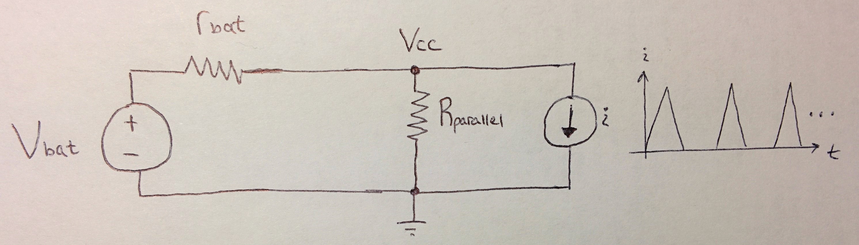
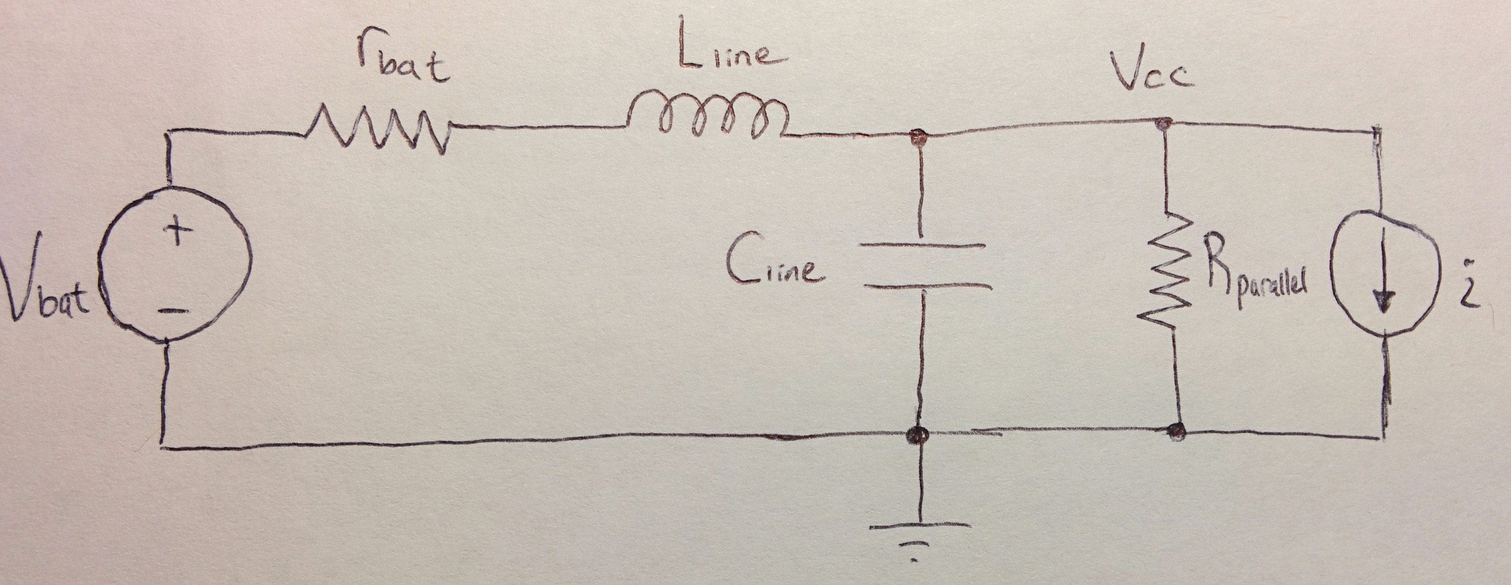
Figure 12 shows a very simplified model of the oscillator circuit from the point of view of the power supply.
In this model the power supply is represented as an ideal voltage source with value Vbat and source resistance rbat.
The LM555 oscillator circuit is modelled as a current sink that draws a short burst of current from the battery once per cycle at a rising edge of the output pulse.
This short burst of current corresponds to the current pulse you measured in Section 4.6.
A resistor with value Rparallel is placed in parallel with the current sink. This resistor draws a small supply current from the battery and simulates the input resistance of the LM555 IC's Vcc pin.
The power supply pin Vcc is shown in the figure.
Figure 12. Simplified equivalent circuit for modelling voltage fluctuation on power line.
In a circuit simulator like SPICE, simulate the circuit shown in Figure 12. Take Vbat= 9 V, rbat = 1 Ohm, and Rparallel = 1 kOhm.
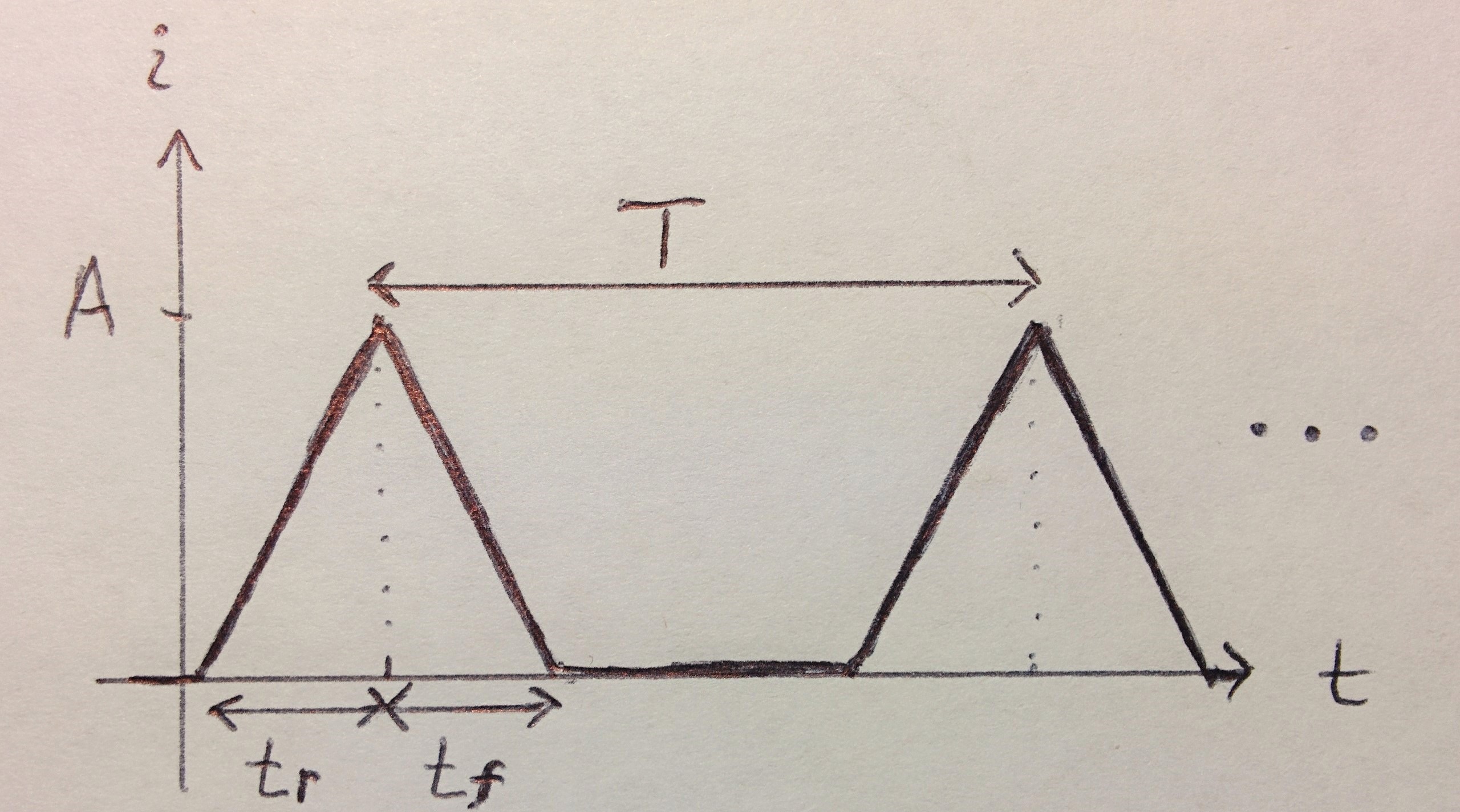
Choose the current source to be triangular pulse train like that illustrated in Figure 13. For this triangular pulse train, choose the amplitude A = 300 mA, the period T = 1.5 us, rise time tr=40 ns,
fall time tf=40 ns
Plot the voltage Vcc over two cycles. Present a screenshot of your SPICE schematic, screenshot of the output waveform, and observations/comments in Slide 20.
Figure 13. The current drawn from IC as a triangular pulse train.
Figure 14 shows a slightly more realistic model of the oscillator circuit from the point of view of the power supply, which now includes
the capacitance (Cline) and inductance (Lline) of the power supply leads.
Figure 14. More complicated equivalent circuit with parasitic line capacitance and inductance.
In SPICE, simulate the circuit shown in Figure 14. Choose the same values as before for Vbat, rbat, and Rparallel, and the triangular pulse train.
Choose Cline = 20 pF and Lline = .4 uH. Plot the voltage Vcc over two cycles.
How does the inclusion of line capacitance/inductance change the waveform from your previous simulation?
How does this waveform compare to the measured waveform of the supply voltage without a bypass capacitor (you measured this in section 4.3)?
Present your answers, screenshot of your SPICE schematic, and screenshot of the output waveform in Slide 21.
Double the line inductance to Lline = .8 uH. How does this change the waveform? Present your answer and screenshot of the output waveform
in Slide 22. When making your comparisons, note that the equivalent circuit model presented here
is only a rough approximation of the circuit you actually measured. It's only meant to model the main features of the switching transients on the power supply line.
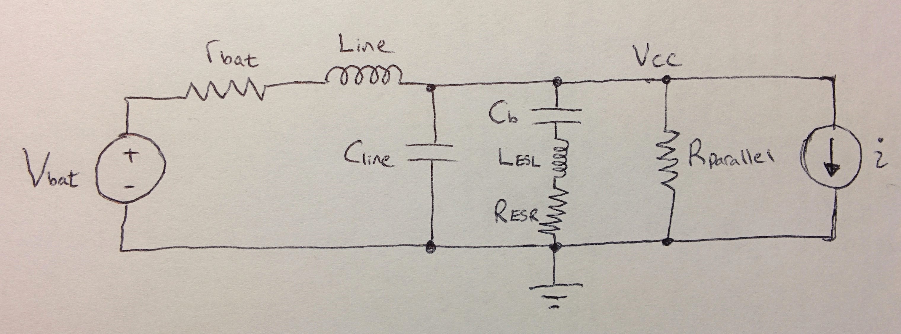
Figure 15 shows a model of the oscillator circuit with a bypass capacitor with capacitance Cb. In this model, the bypass
capacitor has a small inductance LESL and resistance RESR.
Figure 15. Equivalent circuit with bypass capacitor.
In SPICE, simulate the circuit shown in Figure 15. Choose the same values as before for Vbat, rbat, and Rparallel, and the triangular pulse train.
Choose Cline = 25 pF and Lline = .4 uH. For the bypass capacitor, choose Cb=100 uF, LESL = 10 nH, and RESR= 50 milliOhms.
How does the bypass capacitor effect the waveform? Present your answers, screenshot of your SPICE schematic, and screenshot of the output waveform in Slide 23.
Simulate and compare the waveform for five different values for the bypass capacitor: Cb = 470 pF, 0.01 uF, 1 uF, 10 uF, 100 uF.
For all cases, choose the same series inductance and resistance as before (LESL = 10 nH, and RESR= 50 milliOhms).
Present your comparisons in Slides 24 and 25.
Instead of one bypass capacitor as before, try using two bypass capacitors in parallel from the values you have in the step above.
For example, measure the supply voltage using a 470 pF bypass capacitor in parallel with a 100 uF bypass capacitor.
Or you can try two 100 uF capacitors in parallel. Remember, for all capacitors choose the
same series inductance and resistance values as before (LESL = 10 nH, and RESR= 50 milliOhms).
Is there a certain optimum combination you found with respect to suppressing the voltage spikes?
Present your measurements and observations in Slide 26.
Present your conclusions and a summary of what you learned in this lab and how it relates to practical circuit design in Slide 27.
6. References
In this lab, we only scratched the surface when it comes to bypass capacitors and power supply decoupling.
For more information, I recommend the following references:
Application Manual for Power Supply Noise Suppression and Decoupling for Digital ICs,
MuRata Manufacturing Co., Ltd, 2010. Download PDF here.
C.R. Paul Introduction to compatibility engineering, Wiley, 2006.