Circuit a day: Class A BJT common emitter amplifier with voltage-divider-bias
Prepared by Dr. Aaron Scher
[email protected]
Oregon Institute of Technology
Back to Aaron's home page.
Back to Circuit a day.
Notes for future work
The above work is focused on analysis. Future work involves developing a solid design
procedure for designing BJT common emitter amplifiers given competing specifcations and constraints. For now, the list below presents a summary of
some of the interrelated parameters/variables to juggle and optimize
for a given design.
Electrical design
- DC operating point:
- Small signal gain: Voltage gain, current gain, power gain
- Voltage gain: \(A_v = \frac{v_{o}}{v_{i}} = -\frac{(R_L||R_C)}{r_e} \left( \frac{R_i}{R_i+R_s}\right)\) where \(R_i =\) Input impedance \(=R_1||R_2||\beta r_e\), and \(r_e = V_t/I_C \approx .026V/I_C\).
- Impedance: Input/output impedance, VSWR
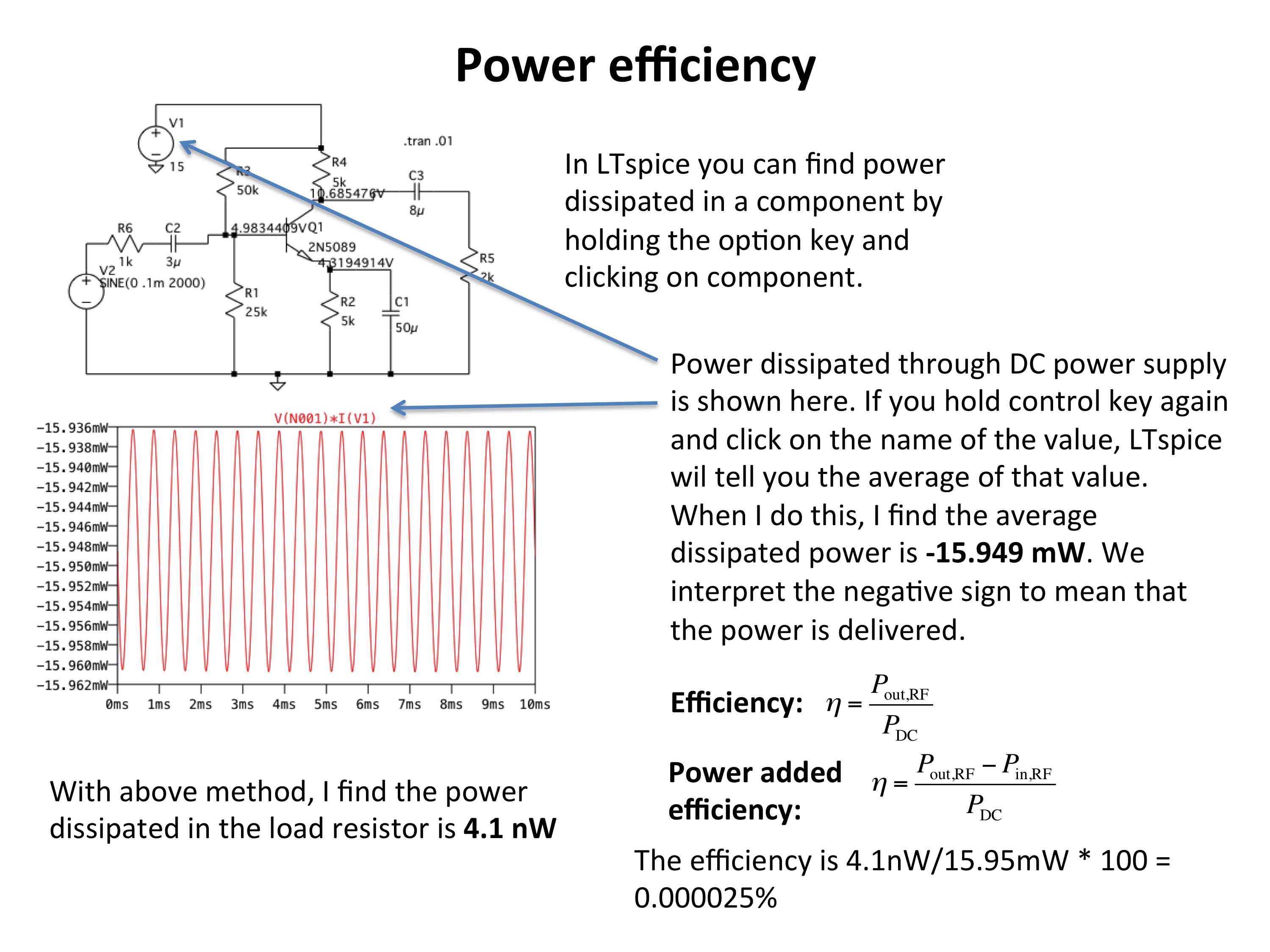
- Power: Power supply voltage, average power drawn from power supply, output AC power, power efficiency
- Frequency response: Miller effect, low/high 3dB cut-off frequencies, gain bandwidth product
- Nonlinearity and distortion: Dynamic range, voltage clipping, intermodulation product distortion (third order intercept IP3), 1 dB Compression point
- Noise: Thermal/shot/flicker noise, transistor noise model, noise temperature, signal to noise ration, noise figure
- Temperature stability
- Oscillation stability: Resilience to unintentional positive feedback
Physical design and project management:
There are also the physical aspects to the design and project management issues, such as:
Shielding/grounding, Electromagnetic compatibility, Packaging, Cost, Part availability, selection and purchasing,
Reading data sheets, Fabrication, Test and measurement, Tolerance, Schedule,
Documentation, Intelectual property, Production